

A garage-based semiconductor enthusiast has achieved something remarkable, demonstrating that advanced chip fabrication is no longer purely the domain of billion-dollar facilities. Matthew Hartensveld, who operates under the moniker Dr. Semiconductor, has successfully manufactured light-emitting diodes in his backyard cleanroom setup. This achievement comes on the heels of his earlier success building functional RAM cells at home, and it raises important questions about the future of personal electronics manufacturing and what this means for consumers.
How the Home Semiconductor Project Took Shape
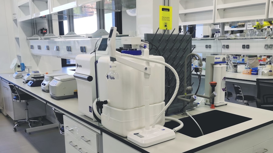
Hartensveld’s journey began with the fundamentals: constructing a backyard cleanroom environment suitable for semiconductor work. After successfully creating RAM cells, he faced the challenge of packaging and processing them, which led him to explore LED fabrication as part of his broader open-source Semiconductor.DIY initiative. The process required specialized equipment and materials that most people would never consider obtainable outside professional foundries.
Starting with gallium nitride deposited on sapphire wafers, Hartensveld needed to etch precise patterns into the material. Industrial facilities use chlorine gas for this step, but such methods are hazardous for home use. Instead, he sourced a high-powered laser from an online marketplace and relocated it to his bathroom to prevent accidental exposure. Without readily available information on using this laser for wafer etching, he relied on trial and error, eventually achieving clean, defined patterns on the sapphire surface.
The Technical Breakthrough
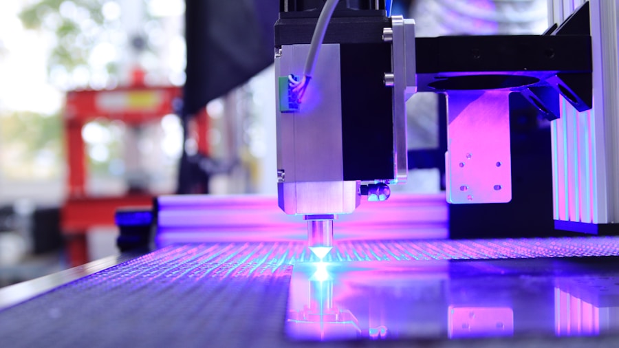
The real innovation emerged when Hartensveld demonstrated that consumer-grade tools could replicate industrial semiconductor processes. After etching patterns, he tested the nascent LED by applying indium contacts and connecting a 9-volt battery. The wafer emitted blue light, proving the concept viable. Creating a fully functional device required additional refinement. He used a two-stage vacuum pump to remove 99.999999 percent of air from a chamber, then deposited nickel and silver contacts using argon plasma deposition. The precision required at each step illustrates why semiconductor manufacturing traditionally demanded institutional resources.
Cutting individual LEDs from the wafer presented another challenge. A standard table saw with thin blades proved inadequate, so Hartensveld returned to his laser tool, focusing the beam to melt away the sapphire substrate in multiple passes. For physical connectors, he employed indium bumps, the same technology found in digital camera sensors. Finally, to create a white LED, he applied a filter made from cerium-doped yttrium aluminum garnet, purchased through online commercial channels, atop his blue LED.
What This Means for Consumers
While Hartensveld’s achievement won’t immediately replace commercial RAM or LED manufacturers, it signals a shift in how accessible advanced fabrication knowledge and tools are becoming. The semiconductor industry has faced supply chain challenges in recent years, making memory and component costs unpredictable for consumers. If more people can replicate fundamental semiconductor processes with consumer equipment, future supply chains may become more resilient and decentralized.
For current buyers, this development has limited immediate impact. Commercial manufacturers maintain massive advantages in scale, consistency, and cost efficiency. However, the feasibility of home semiconductor work could influence education, encouraging younger people to pursue hardware careers and potentially addressing industry talent shortages. Additionally, open-source semiconductor projects may eventually lead to educational tools and kits that demystify electronics for enthusiasts and students.
The broader implication involves the democratization of manufacturing knowledge. When complex processes are documented and shared openly, barriers to innovation decrease. This approach already transformed 3D printing and PCB fabrication from specialized services into accessible hobbies. Semiconductor manufacturing may follow a similar trajectory, though the timeline remains uncertain.
Current Consumer Takeaways
Shoppers shouldn’t expect homemade chips to compete with commercial products anytime soon. Industrial semiconductor fabs produce millions of identical components with specifications measured in nanometers, while Hartensveld’s LEDs are functional prototypes. Manufacturing at scale requires different economic models and quality control systems. However, consumers can appreciate that the technical barriers are lower than previously assumed, and that understanding how memory and components are made enhances appreciation for the devices we purchase.
For the electronics industry, this public demonstration serves as a reminder that innovation doesn’t exclusively occur in corporate laboratories. As semiconductor knowledge becomes increasingly documented and tools grow more accessible, we may see unexpected developments in how chips are designed, manufactured, and distributed. For now, consumers should continue purchasing from established manufacturers, but remain aware that the traditional gatekeeping of semiconductor manufacturing is gradually eroding.









Write Your Review
No reviews yet. Be the first to share your experience!